


A team of scientists from the US Department of Energy’s Ames National Laboratory has developed a new characterization tool that has allowed them to gain unique insight into a potential alternative material for solar cells. Led by Jigang Wang, chief scientist in the Ames lab, the team developed a microscope that uses terahertz waves to gather data about samples of material. The team then used the microscope to study methylammonium lead perovskite (MAPbI3), a material that could replace silicon in solar cells.
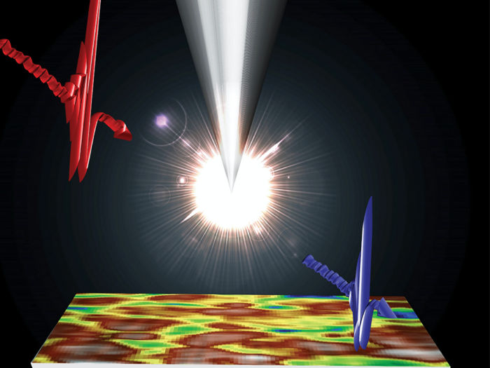
Richard Kim, an Ames lab scientist, explained the two features that make a scanning probe microscope unique. First, the microscope uses the terahertz range of electromagnetic frequencies to gather data about materials. This range is well below the visible light spectrum, and lies between the infrared and microwave frequencies. Second, the terahertz light is directed by a sharp metal tip, which extends the capabilities of the microscope toward the nanoscale of length.
“Normally with wavelength light you can’t see things smaller than the wavelength of light you’re using. With terahertz light, the wavelength is about a millimeter, so it’s pretty big,” Kim explains. “But here we’ve used this sharp metal tip with a curved tip that has a radius of 20 nanometers, and it acts like an antenna to see things smaller than the wavelength we’re using.”
Using this new microscope, the team studied a perovskite material, MAPbI3, which has recently attracted scientists’ interest as an alternative to silicon in solar cells. Perovskites are a special type of semiconductor that conducts an electric charge when exposed to visible light. The main challenge with using MAPbI3 in solar cells is that it degrades easily when exposed to elements such as heat and moisture.
According to Wang and Kim, the team expected MAPbI3 to behave like an insulator when irradiated with terahertz light. Because the data collected on a sample shed light on how light scattered when the material was exposed to terahertz waves, they expected a uniformly low level of light scattering throughout the material. However, they found that light scattering varies greatly along the interfaces between the granules.
Kim explained that conductive materials such as metals have high scattering of light, while less conductive materials such as insulators have lower scattering. The large variation in light scattering observed along MAPbI3 grain boundaries sheds light on the problem of material degradation.
Over the course of a week, the team continued to collect data on the material, and the data collected during that time showed the process of degradation through changes in light scattering values. This information can be useful for improving and processing materials in the future.
“We believe the current study demonstrates a powerful microscopy tool for visualizing, understanding, and possibly mitigating grain boundary degradation, confinement defects, and material degradation,” Wang said. “A better understanding of these issues could enable the development of highly efficient perovskite-based photovoltaic devices for many years to come.”

“Prone to fits of apathy. Zombie ninja. Entrepreneur. Organizer. Evil travel aficionado. Coffee practitioner. Beer lover.”
More Stories
The “One-Man-Show” Next-Gen Update shows how to please players
NASA receives the message via a laser beam from a distance of 226 million kilometers
Upgrade using 20 GPUs and 20 CPUs in testing [Update 3]